Email: sales@telsto.cn
 Telephone: 86-021-6221 2832
 LinkedIn
 Youtube


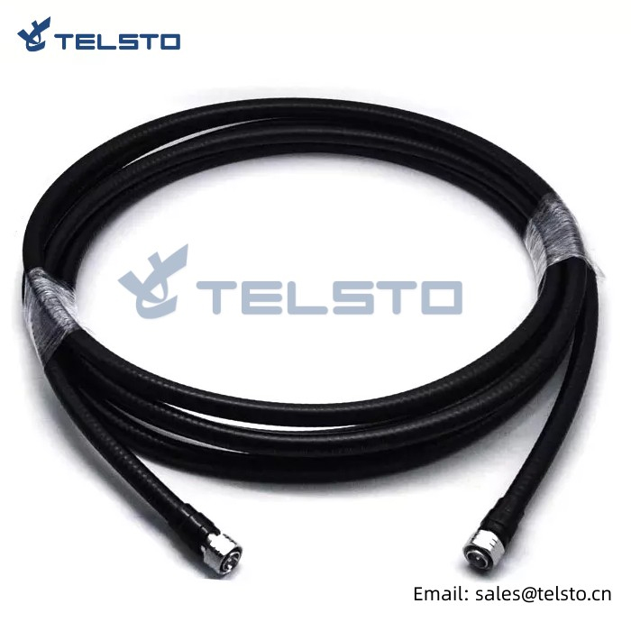
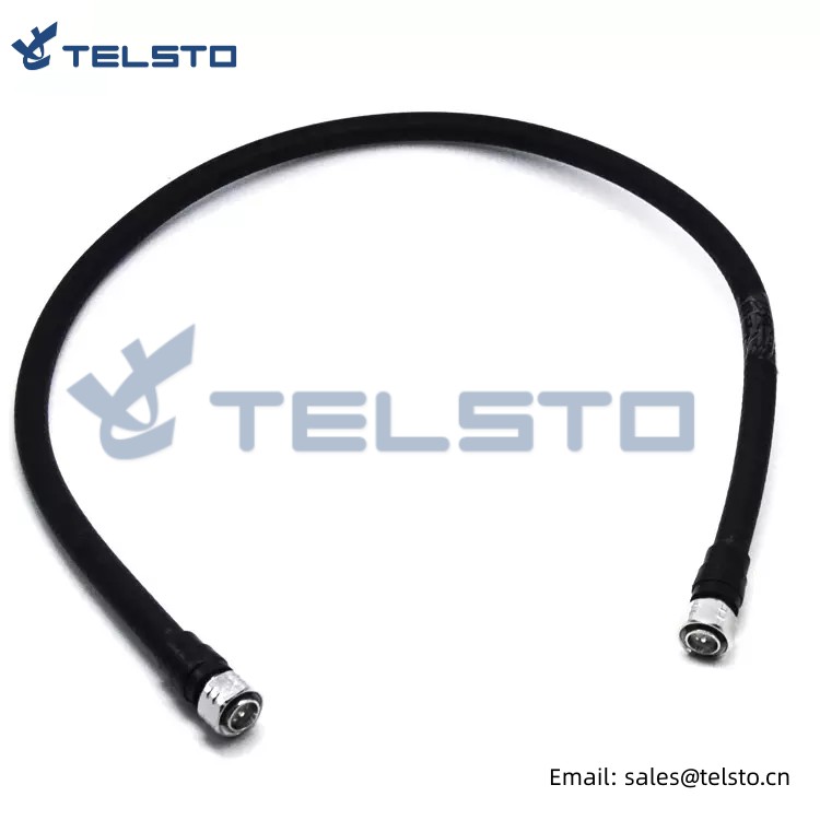
RET AISG 2.0 Cable Assembly Andrew ATCB-B01 Commscope APC-D8 Male to Female PVC Jacket
DESCRIPTIONS
The SFP transceivers are high performance, cost effective modules supporting data-rate of 1.25Gbps and 10KM transmission distance with SMF.
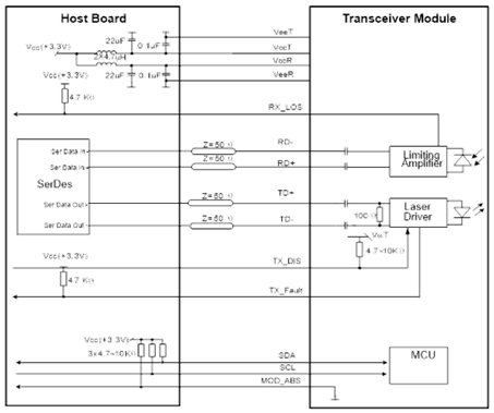
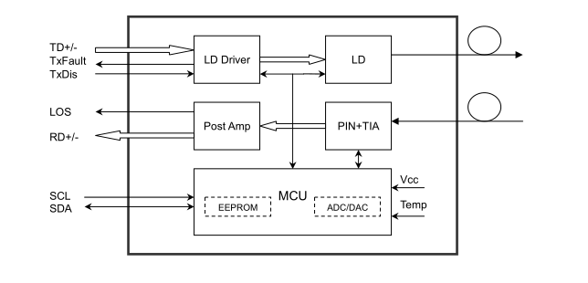
The transceiver consists of three sections: a FP laser transmitter, a PIN photodiode integrated with a trans- impedance preamplifier (TIA) and MCU control unit. All modules satisfy class I laser safety requirements.
The transceivers are compatible with SFP Multi-Source Agreement (MSA) and SFF-8472. For further information, please refer to SFP MSA.
Module Block Diagram
Ordering Information
| Part No. | Data
Rate(optical) |
Laser | Fiber
Type |
Distance | Optical
Interface |
Temp | DDMI | Latch
Color |
| SFP-GE-LX | 1.25Gbps | FP | SMF | 10KM | LC | 0~70℃ | Y | Blue |
| SFP-GE-LX-E | 1.25Gbps | FP | SMF | 10KM | LC | -20~85℃ | Y | Blue |
| SFP-GE-LX-I | 1.25Gbps | FP | SMF | 10KM | LC | -40~85℃ | Y | Blue |
Absolute Maximum Ratings
| Parameter | Symbol | Min | Typ | Max | Unit | Ref. |
| Maximum Supply Voltage | Vcc | -0.5 | 3.6 | V | ||
| Storage Temperature | TS | -40 | 85 | °C | ||
| Relative Humidity - Operating | RHO | 5 | 85 | % | ||
| Relative Humidity - Storage | RHS | 5 | 95 | % |
Recommended Operating Conditions
| Parameter | Symbol | Min. | Typical | Max. | Unit | Notes |
|
Case Operating Temperature |
Top |
0 | - | 70 | ℃ | Commercial |
| -40 | 85 | Industrial | ||||
| Power Supply Voltage | VCC | 3.13 | 3.3 | 3.47 | V | |
| Transmission Distance | TD | - | - | 10 | km | Over SMF |
Electrical Characteristics
| Parameter |
Symbol |
Min | Typ | Max | Unit | Ref. |
| Supply Voltage | Vcc | 3.15 | 3.3 | 3.6 | V | |
| Supply Current | Icc | 303 | mA | |||
| Transmitter | ||||||
| Input differential impedance | Rin | 100 | Ω | 1 | ||
| Single ended data input swing | Vin,pp | 250 | 1200 | mV | ||
| Transmit Disable Voltage | VD | Vcc–1.3 | Vcc | V | ||
| Transmit Enable Voltage | VEN | Vee | Vee+ 0.8 | V | 2 | |
| Transmit Disable Assert Time | 10 | us | ||||
| Receiver | ||||||
| Single ended data output swing |
Vout,pp |
250 | 800 | mV | 3 | |
| Data output rise time | tr | 100 | 175 | ps | 4 | |
| Data output fall time | tf | 100 | 175 | ps | 4 | |
| LOS Fault |
VLOS fault |
Vcc–0.5 | VccHOST | V | 5 | |
| LOS Normal |
VLOS norm |
Vee | Vee+0.5 | V | 5 | |
| Power Supply Rejection | PSR | 100 | mVpp | 6 | ||
Notes:
1. Connected directly to TX data input pins. AC coupled thereafter.
2. Or open circuit.
3. Into 100 ohms differential termination.
4. 20 – 80 %
5. Loss Of Signal is LVTTL. Logic 0 indicates normal operation; logic 1 indicates no signal detected.
6. Receiver sensitivity is compliant w ith power supply sinusoidal modulation of 20 Hz to 1.5 MHz up to specified value applied through the recommended pow er supply filtering network.
Optical and Characteristics
| Parameter | Symbol | Min | Typ | Max | Unit | Ref. |
| Transmitter | ||||||
| Output Opt. Pwr (End of Life) | POUT | -9.0 | -3.0 | dBm | 1 | |
| Optical Wavelength | λ | 1270 | 1310 | 1355 | nm | |
| Wavelength Temperature Dependence | 0.08 | 0.125 | nm/°C | |||
| Spectral Width (-20dB) | σ | 3.5 | nm | |||
| Optical Extinction Ratio | ER | 10 | dB | |||
| Sidemode Suppression ratio | SSRmin | 30 | dB | |||
| Optical Rise/Fall Time | tr/ tf | 100 | 160 | ps | ||
| RIN | RIN | -120 | dB/Hz | |||
| Transmitter Jitter (peak to peak) | 100 | ps | ||||
| Receiver | ||||||
| Average Rx Sensitivity @ Gigabit Ethernet | RSENS3 | -20 | dBm | 2 | ||
| Maximum Input Power | PMAX | -3.0 | dBm | |||
| Optical Center Wavelength | λC | 1260 | 1310 | 1620 | nm | |
| LOS De -Assert | LOSD | -22 | dBm | |||
| LOS Assert | LOSA | -40 | dBm | |||
| LOS Hysteresis | 1.0 | dB | ||||
| Receiver Jitter Generation @1.25Gbps | 160 | ps | 3 | |||
Notes:
1. Class 1 Laser Safety per FDA/CDRH and IEC-825-1 regulations.
2. With w orst-case extinction ratio. Measured w ith a @PRBS=2^7-1 NRZ test pattern, @1.25Gb/s, BER<10-12 .
3. Jitter added by receiver (peak to peak). Measured at –18.0dBm average Rx sensitivity, @PRBS=2^7-1 NRZ test pattern.
Digital Diagnostics
| Parameter | Range | Accuracy | Unit | Calibration |
| Temperature | -40 to 85 | ±3 | ºC | Internal |
| Voltage | 0 to Vcc | ±3% | V | Internal |
| Tx Bias Current | 0 to 100 | ±10% | mA | Internal |
| Tx Output Power | -9 to -3 | ±3 | dB | Internal |
| Rx Input Power | -20 to -3 | ±3 | dB | Internal |
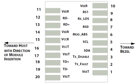
Pin Diagram
Pin Definitions
| Pin | Symbol | Name/Description | Ref. |
| 1 | V
EET |
Transmitter Ground (Common with Receiver Ground) | 1 |
| 2 | T
FAULT |
Transmitter Fault. | 2 |
| 3 | T
DIS |
Transmitter Disable. Laser output disabled on high or open. | 3 |
| 4 | MOD_DEF(2) | Module Definition 2. Data line for Serial ID. | 4 |
| 5 | MOD_DEF(1) | Module Definition 1. Clock line for Serial ID. | 4 |
| 6 | MOD_DEF(0) | Module Definition 0. Grounded within the module. | 4 |
| 7 | Rate Select | No connection required | |
| 8 | LOS | Loss of Signal indication. Logic 0 indicates normal operation. | 5 |
| 9 | V
EER |
Receiver Ground (Common with Transmitter Ground) | 1 |
| 10 | V
EER |
Receiver Ground (Common with Transmitter Ground) | 1 |
| 11 | V
EER |
Receiver Ground (Common with Transmitter Ground) | 1 |
| 12 | RD- | Receiver Inverted DATA out. AC Coupled | |
| 13 | RD+ | Receiver Non-inverted DATA out. AC Coupled | |
| 14 | V
EER |
Receiver Ground (Common with Transmitter Ground) | 1 |
| 15 | V
CCR |
Receiver Power Supply | |
| 16 | V
CCT |
Transmitter Power Supply | |
| 17 | V
EET |
Transmitter Ground (Common with Receiver Ground) | 1 |
| 18 | TD+ | Transmitter Non-Inverted DATA in. AC Coupled. | |
| 19 | TD- | Transmitter Inverted DATA in. AC Coupled. | |
| 20 | V
EET |
Transmitter Ground (Common with Receiver Ground) | 1 |
Notes:
1. Circuit ground is internally isolated from chassis ground.
2. T
FAULT
is an open collector/drain output, w hich should be pulled up w ith a 4.7k – 10k Ohms resistor on the host board if intended for use.
Pull up voltage should be betw een 2.0V to Vcc + 0.3V. A high output indicates a transmitter fault caused by either the TX bias current or the TX output pow er exceeding the preset alarmthresholds. A low output indicates normal operation. In the low state, the output is pulled to
<0.8V.
3. Laser output disabled on TDIS
>2.0V or open, enabled on TDIS
<0.8V.
4. Should be pulled up w ith 4.7k - 10kohms on host board to a voltage betw een 2.0V and 3.6V. MOD_DEF(0) pulls line low to indicate module is plugged in.
5. LOS is open collector output. It should be pulled up w ith 4.7k – 10 kohms on host board to a voltage betw een 2.0V and 3.6V. Logic 0 indicates normal operation; logic 1 indicates loss of signal.
Recommended Interface Circuit